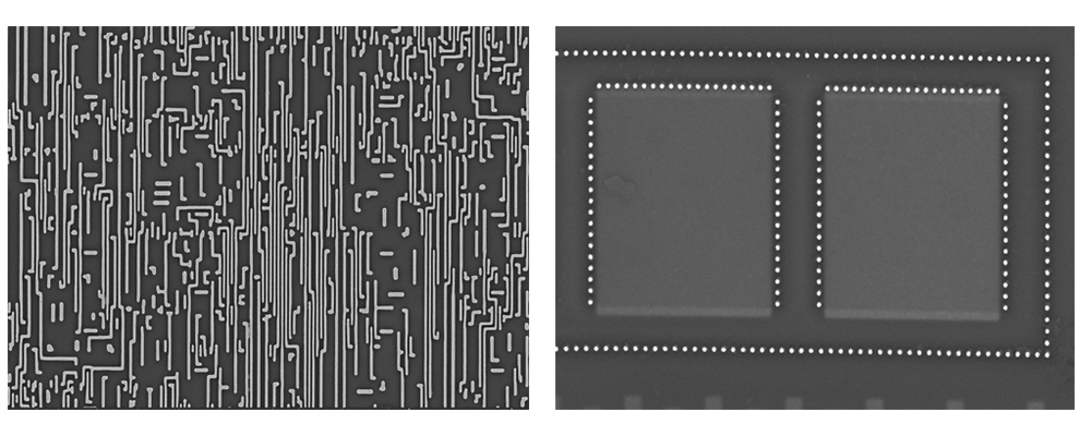
SEM scanning electron microscope
SEM: Scanning electron microscope (SEM) is a large-scale precision instrument used for high-resolution micro area morphology analysis. It has the characteristics of large depth of field, high resolution, intuitive imaging, strong stereo sense, wide magnification range, and the ability to rotate and tilt the tested sample in three-dimensional space. In addition, it has the advantages of rich types of measurable samples, almost no damage or pollution to the original sample, and the ability to simultaneously obtain morphology, structure, composition, and crystallographic information. At present, scanning electron microscopy has been widely used in micro research in fields such as life sciences, physics, chemistry, justice, earth sciences, materials science, and industrial production. In the field of earth sciences alone, it includes crystallography, mineralogy, mineral deposits, sedimentology, geochemistry, gemology, micropaleontology, astronomical geology, oil and gas geology, engineering geology, and structural geology.
As for the application of scanning electron microscopy in the integrated circuit manufacturing industry, it can be mainly divided into five categories:
1. Morphological observation
2. Measurement reference;
3. Cross section observation;
4. Surface observation;
5. EDX analysis (rapid elemental microanalysis, pre scanning, surface scanning)
Semiconductor chip samples

